
The semiconductor manufacturing process leaves no room for errors. Photo: Courtesy of Viettel
The groundbreaking represents more than just another industrial project.
It signals that Viettel and Vietnam as a whole are entering one of the most demanding fields of modern industry, where precision, discipline, and infrastructure standards are among the strictest ever established.
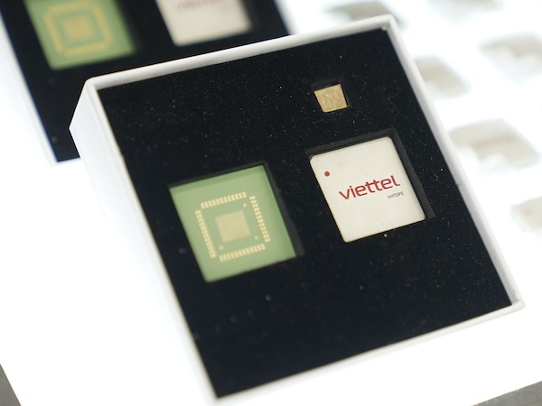
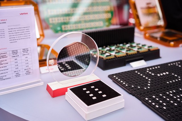
Semiconductor chips are not simple blocks of material but intricate structures made from hundreds of ultra-thin layers, each with unique physical and chemical properties.
To build these layers, a factory must master multiple core technologies.
Every layer goes through seven critical steps, including cleaning, deposition, photolithography, etching, ion implantation, thermal annealing, and planarization.
None of these stages are optional, and no step allows for approximation.
The entire process is closed-loop, sequential, and repeated hundreds of times until the chip is complete.
About 1,000 steps are required to transform a silicon wafer into a semiconductor chip. Photo: Courtesy of Viettel
The process begins with silicon wafers made from nearly perfectly pure silicon crystals.
Semiconductor-grade silicon allows only one impurity atom per billion silicon atoms.
Before entering production lines, wafers must be cleaned to absolute perfection; even a microscopic dust particle can distort circuit patterns and render an entire wafer unusable.
After cleaning comes deposition, where metal or dielectric layers are applied through chemical reactions or physical vapor processes.
Each layer is only atoms thick, requiring ultra-precise control of temperature, pressure, and timing.
Minimal deviations can crack layers or alter their intended properties.

Photolithography, often considered the heart of chip manufacturing, follows.
Engineers must imprint billions of transistors onto an area no larger than a fingernail.
This step relies on some of the most complex and expensive machines ever built, with a single photolithography system costing around US$400 million.
The wafer is coated with a light-sensitive material, then exposed to ultraviolet light through a mask.
Exposed regions dissolve during washing, leaving behind precise circuit patterns.
These patterns guide the next stage: etching, where plasma ions carve microscopic pathways into material layers.
Ion implantation and thermal annealing fine-tune electrical properties, while planarization ensures surface precision for subsequent layers.
Throughout the cycle, constant measurement and inspection, though not forming layers directly, are critical to maintaining yield.
In total, a wafer undergoes roughly 1,000 processing steps.

Vietnamese military-run telecom company Viettel’s semiconductor plant is expected to begin operations in 2027. Photo: Courtesy of Viettel
A single wafer can spend nearly three months circulating inside the factory, traveling tens of kilometers between hundreds of machines.
In large-scale fabs, daily wafer movement can total 240,000 kilometers, equivalent to about six trips around the earth, making logistics optimization a formidable challenge.
Semiconductor fabs are among the most complex industrial systems on earth.
They house cleanrooms spanning several hectares, hundreds of machines costing millions to hundreds of millions of dollars, and operate non-stop.
More than 300 types of materials, gases, and chemicals must be tightly controlled.
Infrastructure demands are equally staggering.
Power consumption can match that of 50,000 households, with near-zero tolerance for voltage drops.
Water must be ultra-pure, containing less than one part per billion of organic carbon, around 2,000 times cleaner than drinking water.
Cleanrooms must meet Class 1 standards, allowing no more than 35 dust particles per cubic meter, far cleaner than surgical theaters. Even vibrations are regulated to levels imperceptible to humans.
These extreme demands explain why only a handful of countries can operate chip fabs.
Therefore, Viettel’s role in leading and operating Vietnam’s first semiconductor fabrication plant is highly significant.
Chip manufacturing is not just about machinery or capital, it is a test of scientific mastery, operational discipline, and industrial rigor at the highest level.
By entering chip fabrication, Vietnam signals a long-term, methodical commitment to becoming a foundational player in the digital economy.

Max: 1500 characters
There are no comments yet. Be the first to comment.